The 8085 Microprocessor is an 8-bit general-purpose microprocessor having 40 pins which is capable of addressing 64kb of Memory.
It works on +5v of single power-supply & can operate at the maximum frequency of 6 Megahertz’s.
Thus, it provides 8-Bit Data-Bus & 16-Bit Address-Bus, it generates 8-Bit I/O Address, so 28=256 i.e only 256-Input Ports & 256-Output Ports can be accessed.
Similarly, it provides 74-Instructions with 5-Different Addressing-Modes.
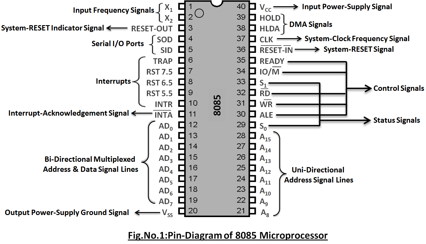
These all 40 Logic Pin-Out Structure of 8085 Microprocessor are divided into 14 Various Groups which are involved into the process of transferring data & executing Instructions in the microprocessor.
These 14 Different Groups in the 8085 Microprocessor can be classified as following:
1) Input Frequency Signals.
2) System RESET Indicator Signal.
3) Serial I/O Ports.
4) Interrupts.
5) Interrupt-Acknowledgement Signal
6) Bi-Directional Multiplexed Address & Data Lines.
7) Output Power-Ground Signal.
8) Uni-Directional Address Lines.
9) Status Signals.
10) Control Signals.
11) Reset Signals.
12) System-Clock Frequency Signal.
13) DMA Signals.
14) Input Power-Supply Signal.
Here, each group helps these entire 40 Logic Pin-Out Structure of 8085 Microprocessor to perform the operations assigned by the 8085 Microprocessor, which are as follows:
1) X1 & X2: ( Pin.No.1 & 2 )
a) These are the 2 clock-input signals which are connected across a crystal RC\LC Circuit of 6MHz Frequency.
b) Whenever the microprocessor requires a clock-frequency of 3MHz, these 2 clock-input pins divides the crystal-frequency into 2 parts in the internal circuitry.
c) Thus, the 1st 3MHz of frequency is supplied to the microprocessor, while the 2nd 3MHz of Frequency is used as an operating frequency to synchronize the operations of 8085 Microprocessor.
d) Here to set the frequency of internal clock generator, X1 can also be an external clock input instead of the First-Input Frequency Signal.
2) RESET OUT: ( Pin.No.3 )
a) This is an Active-High Output System-Reset Indicator-Signal synchronized to the Processor-Clock of Microprocessor & used as an Acknowledgement-Signal to R͞E͞S͞E͞T-I͞N which passes a Low-Sate Signal to R͞E͞S͞E͞T-I͞N to Reset the Whole Internal Structure present in the 8085 Microprocessor along with the Connected-Devices to its Original Initial State.
b) When the 8085 Microprocessor gets the Acknowledgement-Signal from the RESET-OUT to the Reset-Signal R͞E͞S͞E͞T-I͞N for the Operation of System-Reset, the Output of the RESET-OUT goes to High-State & Remains to the High-State as long as the R͞E͞S͞E͞T-I͞N is kept to Low-Sate.
c) Thus, this after receiving the Acknowledgement-Signal from the RESET-OUT, the Reset-Signal R͞E͞S͞E͞T-I͞N resets the HLDA Flip-Flops, the Interrupts Enabled & the Program-Counter to its Original Initial State (i.e 0) & sets the Address & Data Bus along with the Control-Lines Tri-Stated by clearing the entire operands/op-code present temporary in the Memory of Flag-Register & Temporary-Register & then it sends an Acknowledgement-Signal to the RESET-OUT to indicate that the complete 8085 Microprocessor along with the Connected-Devices has been Resetted to its Original Initial State.
d) Thus, to indicate that the complete 8085 Microprocessor along with the Connected-Devices has been Resetted to its Original Initial State, the R͞E͞S͞E͞T-I͞N is goes to High-State & this RESET-OUT goes to Low-State to lasts an Integral-Number of Clock-Periods which is sended to the Processor-Clock of 8085 Microprocessor (i.e CLK) for Synchronization with the Present-Status of the 8085 Microprocessor.
3) SOD (Serial Output Data): ( Pin.No.4 )
a) It is an Active-High Serial Output Data Line used for Serial Data Communication.
b) Generally, it is a 1-Bit Output Port inside the 8085 Microprocessor that is used to write 1-Bit Data to and fro from the Peripheral-Devices.
c) Here, the A6 Bit of the Accumulator which is known as SOE (i.e Serial Output Enable) must be set to 1 to Enable SOD though the Output, by which SOD is Set or Reset as specified by the SIM Instruction.
d) Thus, the Data Writtened is loaded into the 7th bit of the Accumulator when this SIM Instruction (i.e Set Interrupt Mask) is executed to write the SOD Line.
4) SID (Serial Input Data): ( Pin.No.5 )
a) It is an Active-High Serial Input Data Line used for Serial Data Communication.
b) Generally, it is a 1-Bit Input Port inside the 8085 Microprocessor that is used to read 1-Bit Data to and fro from the Peripheral-Devices.
c) Here, 1-Bit Data can also be Externally-Readed and Stored using this SID line.
d) Thus, the Data Readed is loaded into the 7th bit of the Accumulator when RIM Instruction (i.e Read Interrupt Mask) is executed to Read the SID Line.
5) TRAP (RST 4.5): ( Pin.No.6 )
a) It is an Active, Non-Maskable , Vectored Hardware Interrupt which is generally used to enable the 2-Clock Input Pins i.e X1 & X2 by an INTE-FF( i.e Interrupt-Enable Flip-Flop) to indicate the 8085 Microprocessor that the input-power is been received through the Vcc Pin.
b) Since this interrupt has the Highest-Priority among all the Interrupts of the 8085 Microprocessor, it is also used for Some Catastrophic-Events such as Power-Failure/Immediate Emergency Shutoff & Partly-Errors.
c) The Input of this pin is always By-Defaultly Edge as well as Level-Sensitive Triggered, so it makes a Transition from Low (i.e 0) to High (i.e 1) State & it remains High until & unless it is indirectly acknowledged by INTR (sending an interrupting-acknowledgement signal I͞N͞T͞A ) in order to interrupt the 8085 Microprocessor till the end of the execution of an Instruction received by an Externally Interrupting Signal from the Externally-Connected Peripheral Devices, & Thus due to this it avoids False-Triggering caused by some Noise-Susceptibility & Transients.
d) So, Whenever this Interrupt gets activated in the DI/SI State, the 8085 Microprocessor gets an Externally Interrupting Signal from the Externally-Connected Peripheral Devices, which is recognised by its High-to-Low State transition, through which it automatically sets to low & accepts it , Thus after accepting the interrupts, the 8085 Microprocessor sends the active low signal within INTA pin to the Externally-Connected Peripheral Devices which automatically branches to the new ISR where the Vectored-Address of the TRAP Interrupt is stored in the location 0024H of the Program-Counter, & so the 8085 Microprocessor executes ISR addressed in Program-Counter.
e) Thus, after the end of the execution of an Instruction received by an Externally Interrupting Signal from the Externally-Connected Peripheral Devices, the input of this TRAP pin is De-Activated in the middle of the ISR by an I/O Port only after the port is provided the service by the 8085 Microprocessor to the Externally-Connected Peripheral Devices.
f) Therefore, it is a Non-Maskable Interrupt, A Condition may rise to mask it, So it can only be masked by Resetting the Whole 8085 Microprocessor , else there is no other way to mask it even if gets activated in the DI/SI State.
6) RST 7.5: ( Pin.No.7 )
a) It is an Active High Maskable Vectored-Hardware Interrupt which is implemented by a multi-purpose Instruction known as SIM & its status is readed by the RIM Instruction.
b) According to the Priority, it is the Second Highest Priority Interrupt after TRAP pin, which can be enabled by EI Instruction & Disabled/Resetted by DI Instruction, SYSTEM or Processor RESET or after Re-Organization of Interrupts.
c) Thus it is a Positive Edge-Sensitive Triggered Interrupt, it must go to Low-Sate & back to High-State & so it does not need to be maintained high unless and until before a new interrupt or itself is been recognized to initiate it.
d) Thus it consists an In-Built Internal Restart Function; it automatically transfers the Program-Control by saving the contents of the Program-Counter Register into the stack & by jumping to the Specific Memory Vectored Address Location 003CH respectively when it is received.
7) RST 6.5: ( Pin.No.8 )
a) It is an Active High Maskable Vectored-Hardware Interrupt which is implemented by a multi-purpose Instruction known as SIM & its status is readed by the RIM Instruction.
b) According to the Priority, it is the Third Highest Priority Interrupt after TRAP pin, which can be enabled by EI Instruction & Disabled/Resetted by DI Instruction, SYSTEM or Processor RESET or after Re-Organization of Interrupts.
c) Thus it is a Positive Edge-Sensitive Triggered Interrupt, it must go to Low-Sate & back to High-State & so it does not need to be maintained high unless and until before a new interrupt or itself is been recognized to initiate it.
d) Thus it consists an In-Built Internal Restart Function; it automatically transfers the Program-Control by saving the contents of the Program-Counter Register into the stack & by jumping to the Specific Memory Vectored Address Location 0034H respectively when it is received.
8) RST 5.5: ( Pin.No.9 )
a) It is an Active High Maskable Vectored-Hardware Interrupt which is implemented by a multi-purpose Instruction known as SIM & its status is readed by the RIM Instruction.
b) According to the Priority, it is the Fourth Highest Priority Interrupt after TRAP pin, which can be enabled by EI Instruction & Disabled/Resetted by DI Instruction, SYSTEM or Processor RESET or after Re-Organization of Interrupts.
c) Thus it is a Positive Edge-Sensitive Triggered Interrupt, it must go to Low-Sate & back to High-State & so it does not need to be maintained high unless and until before a new interrupt or itself is been recognized to initiate it.
d) Thus it consists an In-Built Internal Restart Function, it automatically transfers the Program-Control by saving the contents of the Program-Counter Register into the stack & by jumping to the Specific Memory Vectored Address Location 002CH respectively when it is received.
9) INTR: ( Pin.No.10 )
a) It is an Active-High, Maskable, Vectored-Hardware General Purpose Interrupt which is implemented for the use of Externally Connected I/O Device to Interrupt the operation performed by the 8085 Microprocessor in the system for transferring Data to and fro from Memory to itself or Vice-Versa.
b) According to the Priority, it is the Fifth Highest Priority Interrupt after TRAP pin & Among all these Interrupts it has the Lowest Priority which is Enabled by EI Instruction (when an Interrupt is received to the 8085 Microprocessor) & is Disabled Immediately after an Interrupt has been received by the 8085 Microprocessor or by SYSTEM or Processor RESET or after Re-Organization of Interrupts.
c) Thus, when an Interrupt is received to the 8085 Microprocessor, the INTR gets activated & it suspends the Normal Sequence of the Instruction where the Program-Counter is inhibited from incrementing & then the 8085 Microprocessor Immediately Disables the INTR by sending an Interrupt-Acknowledgement Signal I͞N͞T͞A to the Externally Connected I/O Device for transferring Data to and fro from Memory to itself or Vice-Versa.
d) Thus, when an Interrupt is Acknowledged by the 8085 Microprocessor through the Interrupt-Acknowledgement Signal I͞N͞T͞A, the branching address depends upon the instruction provided to the 8085 Microprocessor, where during this cycle, a RESTART or CALL Instruction is been inserted to jump to the ISR.
10) I͞N͞T͞A: ( Pin.No.11 )
a) It is an Active-Low, General-Purpose Interrupt-Acknowledgement Signal which indicates that the processor has acknowledged the Externally Connected Peripheral Devices that it has recognized the Interrupt-Signal by an INTR pin & needs the Operation-Code to proceed further.
b) However, this Interrupt-Acknowledgement Signal I͞N͞T͞A has the same timing as RD Signal; it is used instead of RD-Instruction during the Instruction Cycle after an INTR pin is accepted.
c) Thus whenever any interrupt has been recognized through the INTR pin during the interrupt acknowledge cycle, the 8085 Microprocessor generated this Interrupt-Acknowledgement Signal I͞N͞T͞A by making it High & sends this I͞N͞T͞A signal (instead of RD Signal) where the Operation-code provided by the Externally Connected Peripheral-Devices is loaded into the Instruction-Register.
d) Therefore, if the Operation-Code sent by the device implies a Multi-Byte Instruction, Additional I͞N͞T͞A Signals are sent out by the 8085 Microprocessor to complete the Machine-Cycle.
11) AD0-AD7: ( Pin.No.12 to Pin.No.19 )
a) These are the 8 different input & output signal lines which consists of 2 different sets of signal-lines 1) address & 2) data used to carry both, the lower-order 8-bit address of the 16-bit address-bus & the lower-order 8-bit data of the data-bus sent from the microprocessor to the Memory or I/O Device or vice-versa.
b) Thus, these signal-lines are bi-directional, tri-stated, multiplexed & time-shared in nature, so the first lower-order 8-bit address of the 16-bit address-bus is time-shared & multiplexed with the 8-bit data of the 8-bit data-bus, where these multiplexed-bits of the address & data lines present in the AD0-AD7 pin are bi-directionally served as A0-A7 & D0-D7 at the same time, so that it can be used to carry both, the 16-bit address of the 16-bit address-bus & 8-bit data of the 8-bit data-bus.
c) Hence, these address & data lines both consists of a set of maximum 32 lines which are parallel-connected to each other, these lines are de-multiplexed i.e separated using a latch through the ale pin during any op-code fetch operation/execution of any Instruction to save value before the function of the bits changes & then it is passed to the pin which decides wheather the obtained op-code address is for Memory or the I/O Devices.
d) Therefore, during any opcode-fetch / execution of any Instruction, in the first clock-cycle of every machine-cycle, these lines carries the first lower-order of 8-bit address-bits from the 16-bit address-bits to the Memory or I/O Device from the location to be readed or written & during the second as well as third clock-cycle of every machine cycle, it subsequently transfers the 8-bit data from the cpu to the Memory or I/O Device or vice-versa where the cpu may read or write out the data throughout this tri-stated lines which also connects the I/O ports & the microprocessor.
12) VSS: ( Pin.No.20 )
a) It is a type of the Main Output Power-Ground pin which is connected to ground of the VCC pin for avoiding ground-interference.
b) Here, thus it is connected to ground, it not only avoids the ground-interference but it helps the VCC pin to supply the +5v DC of duty-power to the 8085 IC by balancing it voltage and protecting it to get damaged.
13) A8-A15: ( Pin.No.21 to Pin.No.28 )
a) These are 8-different output signal lines which are used to carry out the higher-order 8-bits address of the 16-bit address-bus which is sent from microprocessor to Memory or I/O Device or vice-versa.
b) Thus, these signals are Uni-Directional, non-multiplexed tri-stated & time-shared in nature, they are switched to the high impedance state during HOLD & RESET Mode.
c) Hence, the address-buss consist of 16, 20, 24 or 32 numbers of signal-lines parallely-connected to the 8085 microprocessor which carries the address of Memory or I/O location to be readed or writtened from.
d) Thus, after De-Multiplexing the lower 8-bit address of the 16-bit address-bus from the AD0 to AD7 pin by the ALE pin, these lower-order 8-bit address are joined with the higher-order 8-bit address within the 16-bit address-bus, which is sent to the pin which decides wheather the address is for Memory or I/O Device according to the signal-range.
14) S0 & S1: ( Pin.No.29 & Pin.No.33 )
a) These are the 2 output status signal lines used to indicate the Internal Operation Status of the 8085 Microprocessor to specify the kind of operation to be performed.
b) These 2 output status signal lines are the machine-cycle status-signals sent by the microprocessor itself to distinguish & perform the various types of operation which provides different functions depending on the status-signals given by the microprocessor.
c) Here, the S0 & S1 pins become valid at the beginning of the machine-cycle & remain stable throughout the whole machine-cycle specifying 4 different conditions like HALT, READ, WRITE & OPCODE-FETCH etc.
d) Thus, If S0 = 0 and S1 = 0 it indicates HALT Operation & If S0 = 0 and S1 = 1 it indicates READ Operation; Similarly If S0 = 1 and S1 = 0 it indicates WRITE Operation & If S0 = 1 and S1 = 1 it indicates OP-CODE FETCH Operation.

15) ALE: ( Pin.No.30 )
a) ALE i.e Address Latch Enable is the Active High, Bi-Stated, Output Control-Signal which controls the set of latches/flip-flop in the 8085 Microprocessor to access the External-Memory by De-Multiplexing the Bi-Directional AD0-AD7 pins into the lower-order 8-bit address & lower-order 8-bit data whenever the Microprocessor executes any Read/Write Operation.
b) Thus it is a positive going pulse generated every time while the beginning of any operation/machine cycle in the 8085 Microprocessor, it acts like a common-bus for data-memory & program-memory which indicates whether the multiplexed bus functions as an address bus or a data bus.
c) It is called as Active High Output Control-Signal because whenever the 8085 Microprocessor supplies the active high pulse to this pin, it gets activated & it de-multiplexes the AD0-AD7 pins & tells that when data is present and when address is present on the multiplexed address/data lines.
d) When this ALE is Enabled during any new operation in the 8085 Microprocessor it goes to logic 1 for about ½ clock cycle (i.e ALE=1(High)) & indicates that the address is present in the multiplexed address/data lines & that address is being flown through those multiplexed lines & after the remaining ½ clock cycle if it is disabled during any new operation in the 8085 Microprocessor it goes to logic 1 for about nearly 3 or 4 clock cycles i.e (ALE=0(Low)) it means that the data is present in the multiplexed address/data lines & then data will be flown through the multiplexed lines.
e) Thus, ALE = 1 makes the address latched i.e. latch enable and ALE = 0 makes the address bus disable & making data bus enable.
16) W͞͞R: ( Pin.No.31 )
a) It is an Active-Low, Tri-Stated Output-Control-Signal used to control the writing operations of 8085 Microprocessor.
b) This pin writes the data to the Memory-Location or an I/O Device generated by the 8085 Microprocessor.
c) Here, to write a data into a Memory-Location or an I/O Device, microprocessor selects a device (depending upon the status of IO/M̄ pin & the 2 Status Pins S0 & S1 which decides wheather the data is for either Memory-Location or an I/O Device) & then it transfers the data with data-lines by generating W͞͞R signal.
d) Thus, when the status of IO/M̄ & S1 is 0 & the status of S0 is 1, then the data is writtened to the Memory & when the status of IO/M̄ & S0 is 1 & the status of S1 is 0, then the data is writtened to the I/O Device.
17) R͞D: ( Pin.No.32 )
a) It is an Active-Low, Tri-Stated Output-Control-Signal used to control the reading operations of 8085 Microprocessor.
b) This pin reads the data from the Memory-Location or an I/O Device generated by the 8085 Microprocessor.
c) Here, to read a data from the Memory-Location or an I/O Device, microprocessor selects a device (depending upon the status of IO/M̄ pin & the 2 Status Pins S0 & S1 which decides wheather the data is either in the Memory-Location or an I/O Device) & makes data-bus available & then it generates the R͞D signal to read the data from the selected device.
d) Thus, when the status of IO/M̄ & S0 is 0 & the status of S1 is 1, then the data is readed from the Memory & when the status of IO/M̄ & S1 is 1 & the status of S0 is 0, then the data is readed from the I/O Device.
18) IO/M̄: (Pin.No.34)
a) IO/M̄ i.e Input-Output or Memory is a Output Status-Signal Line by which the 8085 Microprocessor comes to know wheather the operation is to be performed is related to Memory or I/o Device.
b) Here, if IO/M̄=0 (i.e Low) then the microprocessor is acknowledged to perform the operation related to the Memory & if if IO/M̄=1 (i.e High) then the microprocessor is acknowledged to perform the operation related to the I/O Device.
c) Therefore , the operation being performed on the Memory or I/O Device is indicated by the 2 Status-Signal Lines i.e S0 & S1 , if S0=0 and S1=1 then the Status Signals indicates the READ Operation & if S0=1 and S1=0 then the Status Signals indicates the WRITE Operation.
d) Thus, in case of HALT, HOLD & RESET operation, the pin is set to High-Impedance (Z), but only in HOLD & RESET operation, the Status is Not-Defined (X), while in HALT Operation the Status is 0.

19) READY: (Pin.No.35)
a) It is an active-high, input-control signal line used by the microprocessor used to delay the completion of a bus transfer cycle & check wheather the peripheral-devices has completed or is ready to transfer the data or not.
b) This signal is sampled by the 8085 at the falling edge of clock following ALE to synchronize slower peripheral-devices with the faster peripheral-devices by allowing the memory devices to operate at a slower speed than the 8085 Microprocessor.
c) As we know that, the Memory and Peripheral I/O devices has slower response as compared to microprocessors, So before completing the present operation, such a slow peripheral device may not be able to handle further data or control signal from CPU, therefore the READY pin gets Disabled & microprocessor enters into WAIT state and remains in WAIT state until the input at this pin goes high.
d) Thus, in order to handle further data or control signal from CPU, it completes the present operation by making READY high but if READY is Low, then the cycle is extended by one clock, with all lines held steady & then it is sampled again at each of the next falling edges of clock until it is high & after completing the present job, the processor Enables & sets the READY Signal to access the data.
e) Here, if READY Signal from READY pin is high during a READ/WRITE Cycle, it show that the memory or peripheral is ready to send or receiving the data & then the microprocessor completes the operation & proceeds for next operation
f) But if READY Signal from READY pin is low during a READ/WRITE Cycle, then the microprocessor WAITs until the input at this READY pin goes high before completing the READ/WRITE Cycle.
20) R͞E͞S͞E͞T-I͞N: (Pin.No.36)
a) It is an Active-Low Input Reset-Signal used to pass an acknowledgement to RESET OUT Signal Line which indicates that the Whole Internal Structure present in the 8085 Microprocessor along with the Connected-Devices is Resetted to its Original Initial State.
b) Thus, when an Acknowledgement-Signal sended by the RESET OUT is received to the Reset-Signal R͞E͞S͞E͞T-I͞N, the Reset-Signal R͞E͞S͞E͞T-I͞N resets the HLDA Flip-Flops, the Interrupts Enabled & the Program-Counter to its Original Initial State (i.e 0) & sets the Address & Data Bus along with the Control-Lines Tri-Stated by clearing the entire operands/op-code present temporary in the Memory of Flag-Register & Temporary-Register.
c) After this Process is completed, the program-counter starts executing from its initial Memory-location 0000H onwards & this R͞E͞S͞E͞T-I͞N sends an Acknowledgement-Signal to the RESET-OUT to indicate that the complete 8085 Microprocessor along with the Connected-Devices has been Resetted to its Original Initial State.
d) Hence the 8085 Microprocessor is held in the Reset-Condition as long as this signal is been applied to Low-Sate, but after System-Reset Status, the Internal-Register and Flag’s are Un-Predictable.
21) CLK: (Pin.No.37)
a) It is output clock-signal which is used as a system-clock.
b) Sometimes it is necessary for generating clock outputs from microprocessors so that they can be used for other peripheral-devices/digital IC’s in the system to synchronize other devices with the same speed, This is provided by CLK pin by an Internally Operating 3MHz Frequency obtained from the crystally-connected clock-input pins X1& X2, which is stored in this CLK pin.
c) Here, the period of CLK is twice the crystally-connected X1, X2 clock-input period & its frequency is always same as the frequency at which the microprocessor operates.
22) HLDA: (Pin.No.38)
a) HLDA (i.e Hold-Acknowledge) is an output-signal which is used by the 8085 Microprocessor which passes an acknowledgement-signal to HOLD that the HOLD-Request has been received by the 8085 Microprocessor & it will withdraw the buses in the next clock cycle.
b) When HLDA signal goes high, address-bus, data bus, RD, WR, IO/M pins are tri-stated which means they are cut-off from external environment, so the control of these buses goes to DMA Controller & the Control remains at DMA Controller until HOLD is held high.
c) When HOLD goes low, the Hold Request is removed from the HLDA & then the HLDA also goes low and the microprocessor takes control of the buses.
d) Therefore, after the HLDA also goes low the microprocessor takes control of the buses by one-half of clock-cycles.
23) HOLD: (Pin.No.39)
a) HOLD is an Active-High Input Signal Line used to indicate the request sended by the Externally Connected Peripheral I/O Device through the DMA Controllers to the 8085 Microprocessor, which is requesting the 8085 Microprocessor for the use of Address & Data lines to transmit/receive the data from the Externally Connected Peripheral I/O Device to the Internal Memory or Vice-Versa.
b) Whenever an Externally Connected Peripheral I/O Device wants to transmit/receive any data from the Internal-Memory through the 8085 Microprocessor & at that time if the 8085 Microprocessor is using the Address & Data Bus for the Operation related to the Internal Memory, it requests the 2-DMA Controller i.e INTEL 8257 & INTEL 8237 to indicate the request sended by the Externally Connected Peripheral I/O Device to the 8085 Microprocessor, So in response to it the DMA Controller ask for the Buses to the 8085 Microprocessor by making the Output of the HOLD-Pin High which is connected to the Input of HOLD of Microprocessor.
c) Thus, the Internal Processing of the 8085 Microprocessor using the Address & Data Bus for the Operation related to the Internal Memory can be continued, the 8085 Microprocessor receives this High-Output Signal from the HOLD’s input, it relinquishes the control of buses and transfers the control to the Externally Connected Peripheral I/O Device as soon as the current machine cycle is completed & then it sends this High-Output Signal to HLDA to hold the Acknowledgement, that the HOLD-Request has been received by the DMA Controller, by indicating that it has turned the control over buses for other master in the system & making the Address & Data Lines Tri-Sated followed by the RD, WR, and IO/M Lines.
d) Thus, after when the process of transferring the data to and fro from the Externally Connected Peripheral I/O Device to the Internal Memory or vice-versa is completed, the Externally Connected Peripheral I/O Device returns the control of buses back to the 8085 Microprocessor by sending back a Low HOLD Signal.
e) Therefore, the 8085 Microprocessor regain the control of buses after when the HOLD pin gets De-Activated & continues to the Internal Processing of the 8085 Microprocessor where the Operation related to the Internal Memory was been Halted.
24) Vcc: (Pin.No.40)
a) It is a type of the Main Input Power-Supply pin which supplies the External DC Voltage of +5v (i.e 17mA) for the operation of the 8085 Microprocessor.
b) This External DC Voltage of +5v (i.e 17mA) from the Vcc pin is with a Tolerance-Level of 5% & the Maximum Power-Dissipation of 1.5w is connected to this pin only.